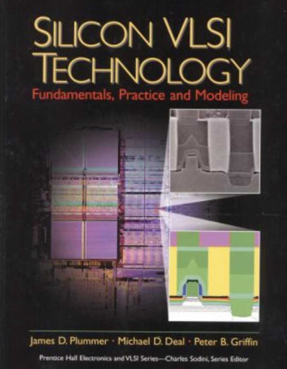
Silcon VLSI Technology
Posted on Wed 16 April 2025 in Reading List

Why I Read This
After finishing up my summer internship researching the deposition of ZnO films with Atomic Layer Deposition, I was fascinated with semiconductor manufacturing technologies; how could we make these incredible modern computer chips? After a long conversation with my advisor, he pointed me to this book to answer all of my questions.
What I Learned
Key Developments that make Today's ICs Possible - Invention of the transistor at Bell Labs. (This started from a search to switch telephone signals with a solid state device. So cool!) - Development of the planar process by Jean Hoerni of Fairchild Semiconductor. This marked the transition from Ge to Si, which was crucial for the industry. SiO2 is easy to deposit on Si and can insulate N and P type regions, allowing more control over electrical properties and smaller gate lengths. - The development of the IC. This really began the transistor revolution and paved the way for Moore's Law.
Semiconductor Physics - "The key to building semiconductor devices and integrated circuits lies in the ability to control the local doping and hence the local electronic properties of a semiconductor crystal." - Nonzero thermal energy causes Si-Si bonds to break in a Si crystal, creating a mobile electron and a "hole" in the crystal structure. These are considered charge carriers becuase they carry electrical currents through the device. - Doping enables us to control and engineer carrier concentrations to tune the performance of a device - Fermi level, probability distribution of electron energy states
PN Junctions - PN Junctions are a result of an equiliobrium between diffusion and electromagentic forces. - Depletion Region: At the junction, there is a large gradient of holes and electrons going from one side to the other. As a reult, they both diffuse across the junction. As they diffuse across the junction however, they leave behind donor and acceptor ions in the Si lattice that essentially try to pull them back through an electromagnetic force. So, the holes and electrons eventually reach a steady state where they are balanced across an electrically neutral depletion region.
Read in Progress! I am actively reading this book when I have time outside of class. I am currently learning many of these semiconduconductor manufacturing techniques through hands-on work experience, and I am excited to continue reading this book and deeply understand the theoretical principles that enable the creation of some of the most advanced technology in the world.